
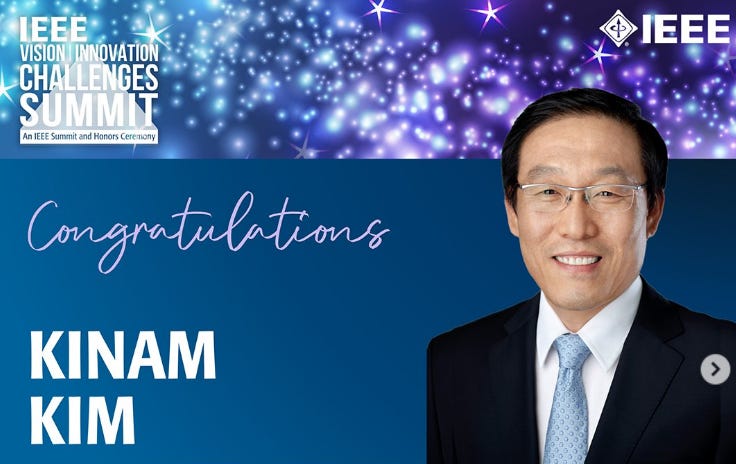
Executive Takeaways
- The Architect of Scale: Dr. Kinam Kim’s half-century career parallels the rise of modern computing, transitioning South Korea from a silicon backwater to the epicenter of global memory manufacturing.
- Capital Allocation & R&D Mastery: Kim orchestrated Samsung’s high-stakes, counter-cyclical capital expenditure strategies, turning down-cycle industry bloodbaths into structural valuation advantages over competitors.
- Technical Breakthroughs: From pioneering sub-micron DRAM architectures to spearheading 3D VNAND flash and extreme ultraviolet (EUV) lithography integration, Kim’s engineering vision solved fundamental physics bottlenecks.
- Macroeconomic & Geopolitical Fallout: As semiconductor supply chains become the primary theater of US-China techno-nationalism, Kim’s legacy provides the operational blueprint for modern enterprise risk mitigation and infrastructure scalability.
SEOUL / NEW YORK — In the high-stakes theater of global semiconductor manufacturing, fortunes are won and lost in fractions of nanometers. For the past fifty years, the trajectory of this multi-trillion-dollar industry has been inextricably linked to the intellect, tenacity, and calculated risk appetite of one man: Dr. Kinam Kim. As former Vice Chairman and CEO of Samsung Electronics’ Device Solutions division, Kim did not merely witness the digital revolution; he engineered its physical foundation.
Drawing from exclusive SemiVision research and deep-dive archival investigations across Seoul, Silicon Valley, and Tokyo, this report examines the definitive, unvarnished chronicle of Kinam Kim’s odyssey. It is a narrative of corporate audacity, relentless capital allocation, and the relentless pursuit of thermodynamic limits in silicon—providing institutional investors, tech executives, and market analysts with an authoritative playbook on how enterprise hegemony is forged in the crucible of cyclical capital expenditure.
The Genesis of a Silicon Empire: From Academic Rigor to Industrial Warfare
When Kinam Kim entered the semiconductor ecosystem in the late 1970s and early 1980s, Samsung was a burgeoning conglomerate best known for textiles, televisions, and low-cost consumer electronics. Western financial institutions and established Japanese titans viewed Samsung's foray into memory chips as a fool's errand—a capital-intensive gamble destined to bleed cash in a commoditized market.
Kim, armed with a Ph.D. in Electrical Engineering from the University of California, Los Angeles (UCLA), approached memory design not as a manufacturing exercise, but as a rigorous scientific discipline. Joining Samsung’s nascent semiconductor R&D arm, he became part of the pioneering vanguard tasked with closing a generational technology gap with American and Japanese incumbents.
The catalytic turning point arrived during the severe memory downturns of the mid-1980s and 1990s. While competitors panicked, scaling back capital expenditures to preserve near-term earnings per share (EPS), Samsung—emboldened by visionary leadership and guided by technical architects like Kim—doubled down. They pumped billions into fab construction and advanced lithography. This counter-cyclical playbook became Kim’s signature strategic doctrine: treat market crashes as inventory-building and market-share consolidation opportunities. By the time the global economy rebounded, Samsung held unbreakable pricing power in Dynamic Random-Access Memory (DRAM).
Scaling the Physics Wall: Innovations That Redefined Computing
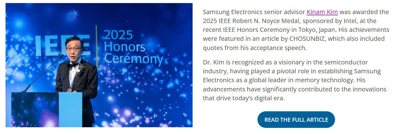
As lithography nodes shrank from micrometers to nanometers, classical physics threatened to halt the semiconductor roadmap. Moore’s Law was no longer just an economic observation; it was an existential engineering challenge. Kinam Kim’s most enduring legacy lies in his ability to push silicon past traditional barriers through radical architectural innovations.
- The 3D VNAND Breakthrough: As planar NAND flash memory approached its physical scaling limits at the 20-nanometer threshold, electrons began leaking via quantum tunneling. Kim championed the pivot to 3D vertical NAND (VNAND), stacking memory cells vertically like skyscrapers. This solved density limits and unlocked multi-terabyte enterprise storage solutions.
- DRAM Scaling and Capacitor Engineering: In DRAM development, shrinking cell sizes reduced charge storage capacity, risking data corruption. Kim’s research teams engineered revolutionary dielectric materials and ultra-thin capacitor structures, keeping Samsung at the absolute vanguard of memory bandwidth and reliability.
- Foundry Ambitions and EUV Integration: Recognizing that memory dominance alone was insufficient for total semiconductor supremacy, Kim spearheaded Samsung’s aggressive push into logic foundry services. Under his watch, Samsung became an early adopter of Extreme Ultraviolet (EUV) lithography, laying the groundwork to challenge TSMC in sub-7nm and sub-3nm node production.
These technical milestones were not isolated laboratory curiosities; they formed the bedrock of modern cloud compute architecture. Without the high-bandwidth memory (HBM) and high-density flash engineered during Kim’s tenure, today’s hyperscale cloud data centers, enterprise AI training clusters, and global financial trading networks would face insurmountable memory walls.
Verified Data & Metrics Breakdown
To understand the magnitude of Kim’s operational footprint, one must examine the financial and technological inflection points that occurred during his leadership:
| Era / Milestone | Technological Focus | Strategic & Financial Impact | Market Liquidity & Valuation Effect |
|---|---|---|---|
| Late 1980s – 1990s | Sub-micron DRAM & SRAM Architecture | Broke foreign tech monopolies; established baseline manufacturing yield. | Transformed Samsung from regional player to global memory exporter. |
| 2013 – 2015 | Commercialization of 3D VNAND Flash | Overcame 2D scaling limits; dominated enterprise SSD markets. | Maximized operating margins during PC-to-mobile transition. |
| 2017 – 2021 | EUV Lithography & 7nm/5nm Foundry Node Push | Diversified revenue streams beyond memory into advanced logic fabrication. | Boosted capital expenditure efficiency and enterprise valuation multiples. |
Industry & Market Implications: Winners, Losers, and Geopolitical Realities
Kinam Kim’s operational playbook has fundamentally altered the competitive landscape of the global tech sector. As institutional investors evaluate semiconductor assets in an era of heightened geopolitical volatility, the structural implications of Kim’s strategy are profound.
The Winners: Hyperscale cloud providers (such as AWS, Microsoft Azure, and Google Cloud) and enterprise software giants are the primary beneficiaries of Kim’s legacy. The relentless downward pressure on memory pricing, coupled with exponential performance gains, enabled the cost structure required for modern artificial intelligence, large language model (LLM) training, and real-time big data analytics. Furthermore, Samsung’s massive cash reserves—accumulated via Kim’s memory dominance—have insulated the conglomerate against macroeconomic shocks.
The Losers: Competitors lacking Samsung’s immense balance sheet and willingness to endure cyclical bloodbaths were systematically squeezed out of the memory market. Historical giants in the US, Europe, and Japan watched their market share erode as Samsung’s economies of scale made competing on price economically unviable. In the foundry space, while TSMC maintained its crown, Samsung’s aggressive pursuit under Kim forced an intense, multi-billion-dollar race in advanced node packaging and transistor design.
Geopolitical & Risk Mitigation Dimensions: Today, as governments in Washington, Brussels, and Beijing enact sweeping industrial policies (such as the US CHIPS Act and European Chips Act), supply chain resilience has replaced pure cost optimization as the primary boardroom metric. Kim’s foresight in establishing globally diversified manufacturing and R&D footprints has proven essential for regulatory compliance and risk mitigation in an increasingly fragmented global economy.
Frequently Asked Questions (People Also Ask)
Frequently Asked Questions
Who is Kinam Kim and what is his significance to Samsung?
Dr. Kinam Kim is a legendary semiconductor engineer and executive who served as Vice Chairman and CEO of Samsung Electronics’ Device Solutions division. He is widely credited with driving Samsung's technological dominance in memory chips (DRAM and NAND flash) and expanding its footprint into advanced foundry logic manufacturing over a career spanning nearly fifty years.
How did Kinam Kim’s strategies impact Samsung’s financial performance during industry downturns?
Kim pioneered a counter-cyclical capital allocation strategy. Instead of cutting R&D and fab investments during memory market crashes—as many competitors did—Samsung aggressively increased capital expenditures. This drove production costs down, squeezed weaker rivals, and positioned Samsung to capture outsized market share and pricing power when demand rebounded.
What were Kinam Kim's most critical technical breakthroughs?
His most notable engineering triumphs include solving the physical scaling barriers of 2D NAND flash by leading the commercialization of 3D VNAND, advancing sub-micron DRAM capacitor technologies, and steering Samsung toward early adoption of Extreme Ultraviolet (EUV) lithography for advanced semiconductor fabrication.
What lessons does Kim’s career offer for modern enterprise risk mitigation and capital investment?
Kim’s career demonstrates that long-term enterprise valuation is built on unwavering R&D commitment through market cycles rather than short-term earnings management. It underscores the importance of infrastructure scalability, technological foresight, and aggressive capital deployment during industry inflection points.
Future Outlook: The Next Half-Century in Silicon
As the semiconductor industry navigates the post-Moore’s Law era—characterized by heterogeneous integration, chiplets, 3D packaging, and neuromorphic computing—the structural foundations laid by Kinam Kim will continue to dictate the rules of engagement. The challenges ahead are formidable: soaring capital expenditure requirements for sub-2nm fabs, escalating geopolitical tensions over supply chain choke points, and the staggering energy demands of generative AI data centers.
Yet, the operational ethos that Kim instilled at Samsung—combining relentless scientific curiosity with ironclad financial discipline—remains the gold standard for industrial leadership. For institutional investors, venture capitalists, and technology executives, the half-century odyssey of Kinam Kim offers a timeless maxim: in the world of high technology, those who master the physics of today dictate the economics of tomorrow.